Table Of Content
The footprint defines the precise dimensions for things like component length and width, number of pins, pin layout, and diameter of through holes. If your PCB is already assembled, you can use a thermal imager to measure the heat signature of the PCB while it is operating. This can help you to identify components or sections that are emitting excessive heat. For ease of access, it is usually a good practice to place any power supply connections or other input/output connections near the PCB edge. Aligning similar components in the same direction is also a good practice. These topologies are used to describe how sub-circuits are connected to a power supply sub-circuit (C1).
10 Fundamental Rules of High-Speed PCB Design, Part 5 - I-Connect007
10 Fundamental Rules of High-Speed PCB Design, Part 5.
Posted: Sun, 21 Apr 2024 03:14:12 GMT [source]
Working with a Connection Object on a PCB in Altium Designer
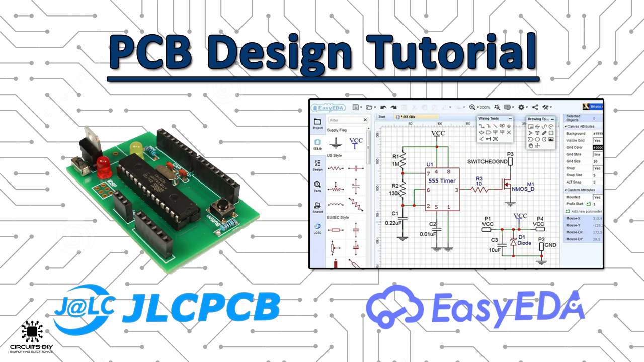
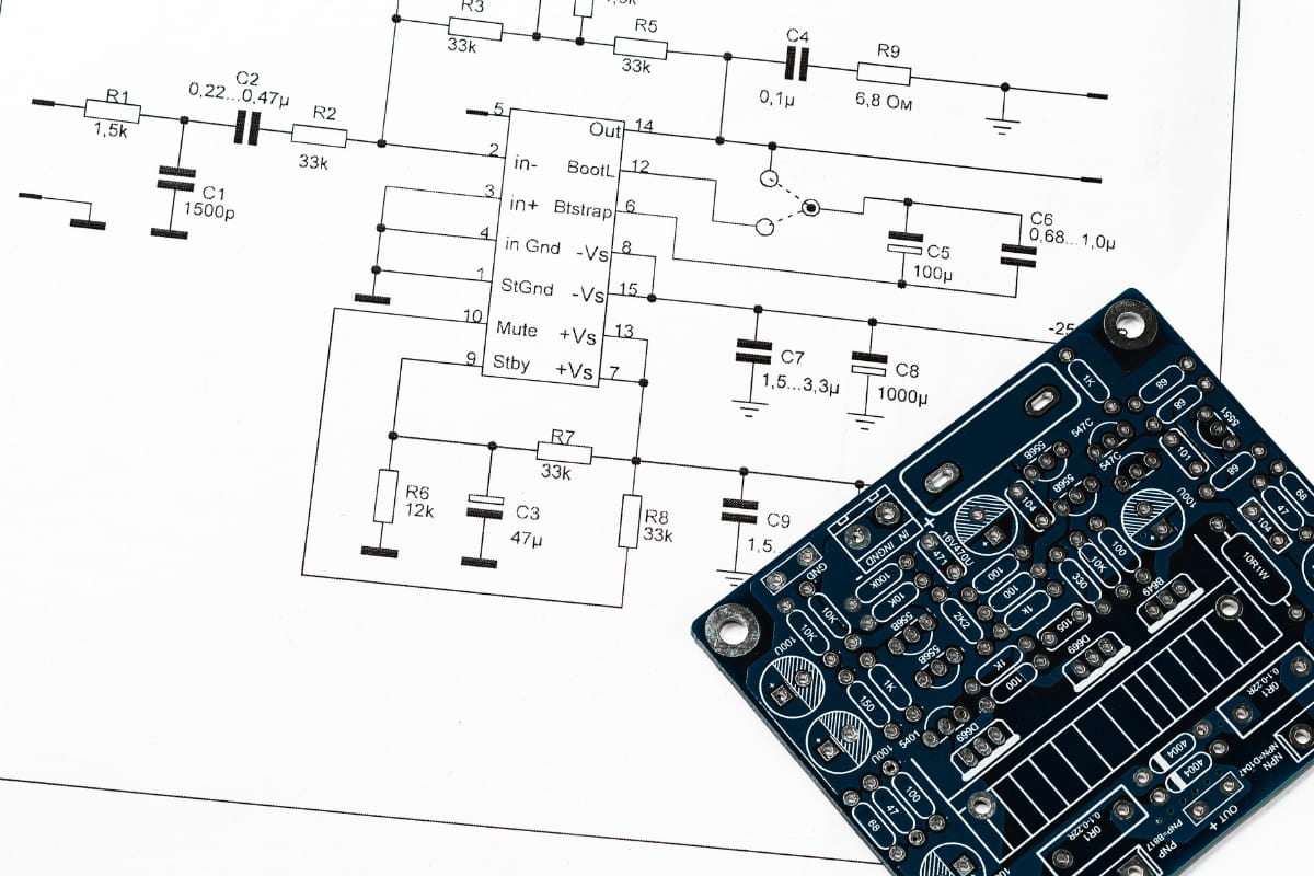
Learning how to design a PCB layout can be separated into two major tasks. Before you create a layout, you need to create a schematic that includes the components your system needs and shows connections between them. Once your schematic is created and successfully verified, you can transfer your design to a PCB layout, which defines the physical architecture of your board. This may seem simple enough, but each task requires several interdependent steps.
Source Data Fig. 3
These tools are used by engineers to design, test, and optimize PCBs for electronic devices. PCB design software can help engineers produce quality boards efficiently and to a high degree of accuracy. Once the schematic is complete, the next step is to create a PCB layout design. This includes the placement of components, the routing of traces, and the placement of vias and holes. Your preferences here should be guided by the design for manufacturing (DFM) specifications of your PCB manufacturer. If you already defined your PCB DFM requirements as design rules (see Step 5), Altium Designer will automatically check these rules as you place vias, drill holes, pads, and traces in your layout.
ADDING A SCHEMATIC TO THE CIRCUIT BOARD PROJECT
With such diverse key stake holders being both internal and external, organized complexity demands multi-discipline collaboration and integration. Refer to Figure 2 for an example of today’s system level connectivity – organizational complexity. For example, it’s not uncommon to see offers of 5 copies of your board for less than $5 USD! When you’re finished drawing your PCB design, you need to get the design made. You could etch your PCB at home, but my preferred way is to just order a PCB from one of the many PCB manufacturers out there. And once you’ve gone through these steps one time, the second time everything is much easier.
The ground connection can be to a battery on the board or to an external power supply. No matter how that connection is made, that ground connection then needs to be supplied to all other components in the PCB. By far, the easiest way to do this is with a ground plane, where one of the layers in the PCB is used for ground with a large sheet of copper covering the entire layer. After you’ve learned about the manufacturing process, as well as some of the standard capabilities found from PCB fabricators, it will be much easier to understand some of the limits imposed in design rules. Most DFM problems relate to the size of copper features in the PCB, or the clearance between different features.
Schematic Capture
It’s important to work with engineering experts from the beginning so that you can design for manufacturability and ensure a final, cost-effective product that works efficiently and effectively. It’s easy to get overwhelmed toward the end of your design project as you scramble to fit your remaining pieces together for manufacturing. Double and triple-checking your work for any errors at this stage can mean the difference between a manufacturing success or failure. If the design will be assembled by hand, such as with solder paste and a heat gun, then the PCB layout might need thermals to trap enough heat near the pad and prevent tombstoning.
Step 5: Defining PCB Board Design Rules and DFM Requirements
Downloading PCB design software follows a similar process to any regular software download, but it’s best to check the specific process of your chosen program as it can vary. On the flip side, it doesn’t boast the same sleek design and intuitive environment of some other PCB software, so it can take a fair while to get used to. However, it does offer a range of great tools for making PCB layouts, and there are some helpful learning resources to get started with.
Altium Designer Makes Design Rules Work for You
In this tutorial, I’ll walk you through the process of designing a PCB layout and getting it printed by a custom PCB manufacturer. The performance of your circuit will depend greatly on how it’s laid out on the PCB, so I’ll give you lots of tips on how to optimize your design. Breadboards are great for prototyping circuits, but they aren’t so good for actually using the thing you’re building. At some point, you’ll probably want to make a project more permanent.
Version control PCB Design with Git « Adafruit Industries – Makers, hackers, artists, designers and engineers! - Adafruit Blog
Version control PCB Design with Git « Adafruit Industries – Makers, hackers, artists, designers and engineers!.
Posted: Wed, 06 Dec 2023 08:00:00 GMT [source]
When soldering by hand, it can be difficult to maintain consistent heating across the component leads, and a thermal connection can help prevent a tombstoning defect. Whether the thermal gets applied to the pour region depends on how the PCB will be assembled. When a net is analyzed and a connection line added, the software automatically adds it based on the topology of the net.
For dissipating heat way from SMD components, thermal via arrays are commonly used. Some components generate heat when an electric current flows through them. Potential heat sources may include voltage regulators, op-amps, transistors, and even copper traces and vias. You might need to employ heatsinking to remove excess heat from these devices. A daisy chain topology is when one sub-circuit is connected to the next in a chain until the circuit is returned to ground. A daisy chain topology reduces the length of traces and saves space on the PCB.
You should also calculate how much current will flow in your circuit. This will help you determine what trace width to use so that current can flow without shorting out a trace. Use this trace width calculator to find the ideal trace width for a particular current. Explore comprehensive digital electronic design solutions that will bring your digital transformation to life. Centralize and streamline your library management workflow with templates, lifecycles, and where-used capabilities, plus monitor for issues like supply chain risks or inaccurate part details.


No comments:
Post a Comment